Abstract 1. High activity oxygen evolution catalyst IrOx/SrIrO3 (AhighlyactiveandstableIrOx/SrIrO3catalystfortheoxygenevolutionre...
1. High activity oxygen evolution catalyst IrOx/SrIrO3
(A highly active and stable IrOx/SrIrO3 catalyst for the oxygen evolution reaction)
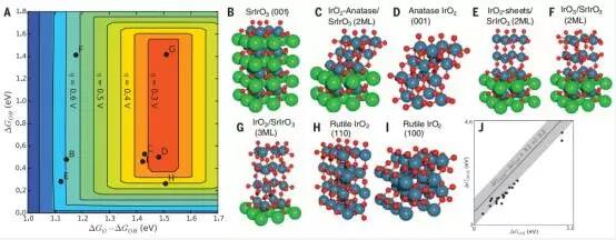
Oxygen electrochemistry plays an important role in renewable energy technologies such as fuel cells and electrolyzers, but the slow kinetics of oxygen evolution (OER) limits the performance and commercial applications of these devices. Recently, the Jaramillo research team at Stanford University in the United States obtained the IrOx/SrIrO3 oxygen evolution catalyst by partial leaching of Sr on the surface of SrIrO3 film during electrochemical process. This catalyst has an overpotential of only 270-290 mV at a current density of 10 mA/cm2 in an acidic environment and can be maintained for 30 hours. Density functional theory calculations also indicate the formation of high active surface of IrO3 or anatase IrO2 during Sr precipitation. The performance of their synthesized IrOx/SrIrO3 oxygen evolution catalysts exceeds the known IrOx and RuO= systems. (Science DOI: 10.1126/science.aaf5050)
2. Tetrapyrrole functionalized graphene boundary
(Fusing tetrapyrroles to graphene edges by surface-assisted covalent coupling)
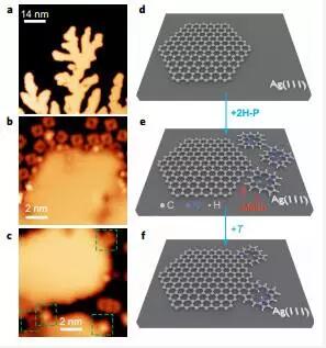
The covalent linkage of precursor molecules with surface aids makes it possible to synthesize low-dimensional nanostructures such as graphene nanoribbons. Methods of constructing functionalized multi-component systems often involve the lateral linking of organic heterogeneous molecules to graphene. Recently, He et al. reported dehydrogenation of monoporphyrin to the graphene edge on the same metal substrate. This covalent linkage becomes visualized at sub-molecular resolution by scanning probe technology, revealing the shape and electronic characteristics of the bond. Different configurations can be achieved by heat-treating two pyrrole rings and adjusting the orientation of the monomers to the graphene boundary. Moreover, they successfully achieved macrocyclic metal substitution and axial conjugate ligation by interaction with a metal substrate. This process combined with the synthesis of graphene nanostructures can create complex functional material systems. (Nature Chemistry DOI: 10.1038/NCHEM.2600)
3. Metal tin quantum sheets for high efficiency CO2 reduction
(Metallic tin quantum sheets confined in graphene toward high-efficiency carbon dioxide electroreduction)
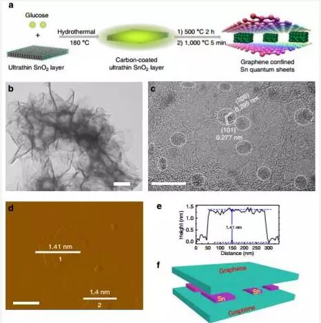
The ultra-thin metal sheet is easily oxidized and can be used as a highly active CO2 electrochemical reduction catalyst. The research group of Academician Xie Yi of the University of Science and Technology of China constructed a model of graphene-limited ultra-thin high-activity metal sheets, and demonstrated it by using graphene-limited high-activity metal tin quantum sheets as an example. The high active electrochemical area makes it exhibit 9 times higher CO2 adsorption capacity than bulk metal tin, while the highly conductive graphene promotes the electron transfer process of CO2 conversion to free radical ions. The X-ray absorption fine structure spectrum reveals a reduced Sn-Sn coordination number. In addition, a decrease in the hydroxyl ion adsorption potential of 0.13 V indicates that limiting the quantum sheet to graphene effectively stabilizes the CO 2 radical ion. This result provides a new idea for designing an effective and stable catalyst for the synthesis of electrolytic fuels. (Nature Communications DOI: 10.1038/ncomms12697)
4. Van der Waals heterojunction is used as a two-terminal floating gate memory
(Two-terminal floating-gate memory with van der Waals heterostructures for ultrahigh on/off ratio)
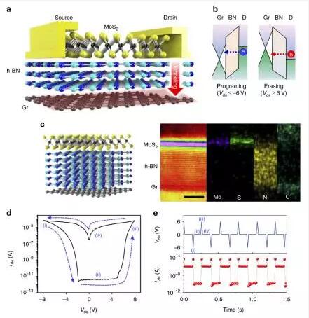
The concept of non-volatile memory replacing traditional flash memory is hampered by low material reliability and high off current, and the use of a thick, rigid oxide layer in flash memory further limits its vertical extension. Vu et al. propose a two-terminal floating gate memory which is a tunnel random access memory made up of a single layer of molybdenum disulfide, hexagonal boron nitride (hBN), and single layer graphene stacked vertically. The device utilizes a two-terminal electrode to achieve current flow in the molybdenum disulfide channel, and is used to charge and discharge the graphene floating gate through the hBN tunneling barrier. The memory device exhibits an ultra-low open current of 10-14 A, which also gives it an ultra-high switching ratio of over 109, which is about 103 times higher than other two-terminal memories. In addition, since there is no thick rigid oxide material which makes it highly flexible (419%), it can be used for flexible electronic devices. (Nature Communications DOI: 10.1038/ncomms12725)
5. Graphene package realizes two-dimensional GaN
(Two-dimensional gallium nitride realized via graphene encapsulation)
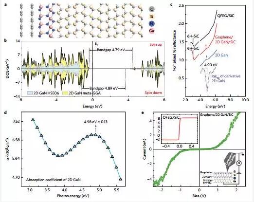
The spectrum of two-dimensional (2D) layered materials provides a good platform for studying new phenomena in condensed matter physics. Among these materials, layered hexagonal boron nitride (hBN) has a wide energy gap (about 5.0-6.0 eV), indicating that two-dimensional nitride is an important material for developing two-dimensional devices. However, there is still a certain gap between experimental and theoretical predictions of two-dimensional nitrides other than boron nitride. Zakaria et al. synthesized two-dimensional gallium nitride (GaN) by epitaxial graphene by migration enhanced encapsulation growth (MEEG) technique. Combined with theoretical prediction and experimental verification, it was found that the atomic structure of two-dimensional GaN synthesized by MEEG growth is obvious with the existing theory. different. They also pointed out that graphene plays a key role in stabilizing the direct energy gap of the two-dimensional snap structure (nearly 5.0 eV). This result provides the basis for the discovery and stabilization of two-dimensional nitrides that are difficult to prepare by conventional synthetic methods. (Nature Materials DOI: 10.1038/NMAT4742)
6. Acoustic topological insulator and strong one-way sound transmission
(Acoustic topological insulator and robust one-way sound transport)
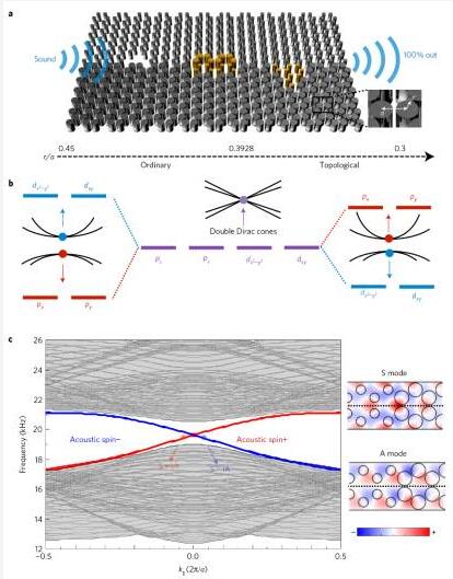
The topological design of the material gives it a topological symmetry to facilitate the transmission of backscattered waves. However, in aeroacoustics, the inherent longitudinal nature of sound polarization makes it impossible to achieve band inversion by conventional spin-orbit interaction mechanisms. Recently, He et al. reported an acoustic energy band reversal at the double Dirac cone and provided an experimental example of an acoustic topological insulator. By controlling the hopping interaction of adjacent atoms in this new topology material, the acoustic quantum spin Hall effect is successfully demonstrated, which is characterized by èµ spin-dependent unidirectional boundary sound transmission. This result provides a new way for experimental exploration of topological phenomena and related applications. (Nature Physics DOI: 10.1038/NPHYS3867)
7. Highly adjustable spin-charge conversion on the oxide interface
(Highly efficient and tunable spin-to-charge conversion through Rashba coupling at oxide interfaces)
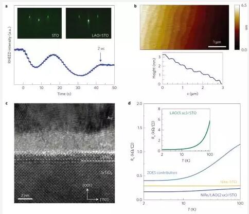
Spin-orbit interactions cause the motion of electrons to couple their spins. Therefore, the charging current forms a lateral spin current (spin Hall effect, SHE) through a material with strong spin-orbit coupling, and vice versa (inverse spin Hall effect, ISHE). The emergence of SHE and ISHE based on the charge-spin mutual conversion mechanism provides a variety of new spintronic functions and devices, some of which do not require any ferromagnetic materials. However, the mutual conversion efficiency of SHE and ISHE is rarely more than 10% as a whole, and the interface and low-dimensional effects ubiquitous in the spintronic heterostructure and mesoporous structure are not utilized. Lesne et al. used the interface-driven spin-orbit coupling mechanism, the Rashba effect, in the oxide two-dimensional electronic system (2DES) laAlO3/SrTiO3 to achieve an unprecedented efficiency of spin-charge conversion efficiency. By the spin excitation, a spin current which can be modulated by the gate voltage is injected from the NiFe film into the oxide 2DES, and the obtained charging current is detected. Lesne et al. discussed the magnitude and gate dependence of the effect based on the electronic structure of 2DES and emphasized the importance of long scattering time for achieving efficient spin-charge interconversion. (Nature Materials DOI: 10.1038/NMAT4726)
8. Non-destructive imaging of buried electronic interfaces
(Non-destructive imaging of buried electronic interfaces using a decelerated scanning electron beam)
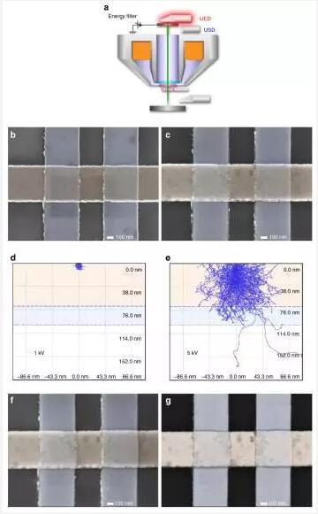
Recent advances in nanotechnology have enabled the fabrication of atomic abrupt interfaces in multilayer junctions, allowing the number of transistors to be added to the processor. However, local defects present in the junction render it difficult to achieve uniform electron transport across the interface, resulting in localized heat generation and reduced mobility. To date, the evaluation of the uniformity of the knot has primarily been made using a cross-sectional TEM, and the slicing and grinding steps required for this process potentially introduce additional damage and deformation. Therefore, it is necessary to develop a non-destructive method. Atsufumi et al. demonstrated a non-destructive technique for mapping buried junction properties using scanning electron microscopy. By controlling the electron beam energy, they show a contrast imaging of the local junction resistance at a certain depth. This technology can be applied to existing semiconductor and metal devices, as well as to all buried junctions of organic devices. (Nature Communications DOI: 10.1038/ncomms12701)
HIPS Sheet has high impact strength and toughness, can be colored at will, molding processability, chemical resistance, and electrical properties are also good. Rubber modified polystyrene has greatly improved impact strength and toughness. At present, it has partially replaced expensive ABS materials.
It can be widely used in: light boxes, advertising, blister, screen printing, model materials, insulating materials, etc. The thickness range is 0.2~9.0mm. The width is within 1500mm, the length is arbitrary, the conventional color is white, other colors can be customized, the size is made according to the data provided by the customer, and the accuracy is high
1. HIPS Sheet for advertising printing
2. HIPS Sheet for screen printing ,digital printing,UV Printing
3.HIPS Sheet for vacuum forming
4.HIPS Sheet for thermoforming yoghourt cup
HIPS Sheet
Polystyrene Acrylic Sheet,PS Plastic Sheets,Polystyrene Sheets Ps
SHENZHEN XIONGYIHUA PLASTIC INSULATION LTD , https://www.xyhplastic.com